GPU Clock Throttling: Why You Never Reach Peak FLOPS
Originally published in Chinese on Zhihu, December 21, 2024.
Background
The three figures that matter most when selecting GPU hardware are compute, memory capacity, and memory bandwidth. Of these, tensor-core peak throughput (FP32/FP16/FP8) is the headline number for judging how much a compute-bound workload can be accelerated. In practice, even cuBLAS and cuDNN kernels fall short of that rated peak, and how far short depends on the shape of the GEMM or convolution. Which raises a question worth sitting with:
Setting aside operators that are simply too small — those with low arithmetic intensity — when an operator's theoretical arithmetic intensity is high enough, does falling short of peak mean the vendor's kernel implementation is not good enough?
The answer sets the ceiling on what optimization work can achieve on a given piece of hardware. Misjudge that ceiling and entire directions of optimization effort are aimed at the wrong thing.
The culprit turns out to be power — a constraint that is easy to overlook until you measure it. The rest of this section introduces the hardware power figures that govern GPU performance.
Clock Frequency
GPU clock frequency directly determines CUDA kernel performance. Clocks are visible through nvidia-smi:
(base) [root@hostname]# nvidia-smi -q -d CLOCK -i 0     # A800 PCIE
Attached GPUs                             : 8
GPU 00000000:35:00.0
    Clocks
        Graphics                          : 1410 MHz
        SM                                : 1410 MHz
        Memory                            : 1512 MHz
        Video                             : 1275 MHz
What these mean:
- Core clock (graphics clock) — the base operating frequency of the GPU core itself, i.e. how fast the graphics processing unit runs.
- SM (streaming multiprocessor) clock — on NVIDIA GPUs this is the same as the graphics clock, since the SMs are the core compute units.
- Memory clock — the operating frequency of device memory, which determines memory bandwidth. The relationship between memory clock and bandwidth on typical cards is below.
Taking the 4090:
GB/s, and dual-channel GB/s.
| Name | Memory clock | Memory interface width | Memory bandwidth | SM clock |
|---|---|---|---|---|
| T4 | 5000 MHz (GDDR effective clock) | 256-bit | 300 GB/s | 1590 MHz |
| A10 | 6251 MHz (GDDR effective clock) | 384-bit | 600 GB/s | 1695 MHz |
| A800 | 1512 MHz | 5120-bit | 1935 GB/s | 1410 MHz |
| 4090 | 10501 MHz (GDDR effective clock, 2625 MHz base) | 384-bit | 1008 GB/s | 3105 MHz |
- Video clock — the clock for the encode/decode engines (NVENC/NVDEC), specific to video codec work.
For datacenter GPUs in AI workloads, the two that matter are the SM clock and the memory clock; they bound the efficiency of every operator on the device.
Clocks can be locked through nvidia-smi:
# Query current clocks
nvidia-smi -q -d CLOCK

# List supported clock rates
nvidia-smi --query-supported-clocks=timestamp,gpu_name,gpu_uuid,memory,graphics --format=csv -i 0

# Lock clocks
nvidia-smi -i [GPU_ID]  --lock-gpu-clocks=<core_clock_rate> (-lgc)
nvidia-smi -i [GPU_ID]  --lock-memory-clocks=<memory_clock_rate> (-lmc)

# Reset clocks
nvidia-smi --reset-gpu-clocks (-rgc)
nvidia-smi --reset-memory-clocks (-rmc)
Note that this lock is not a hard constraint. Under heavy load, or where an adaptive frequency-scaling algorithm is in play, a clock that reports as locked may not hold.
Thermal Design Power (TDP)
Wikipedia defines TDP as the maximum heat a component — CPU, GPU, or SoC — generates in normal operation, and which its cooling system is designed to dissipate. Computer Architecture: A Quantitative Approach frames it as sustained power:
TDP is neither peak power (which is often 1.5× higher) nor the actual average power drawn during a given computation, which may be lower. When sizing a power supply for a system, the supply is typically rated above TDP, and the cooling system is designed to dissipate at least TDP. If cooling is inadequate, junction temperatures inside the processor can exceed their maximum, causing device failure or permanent damage. Because maximum power can exceed the long-term average TDP defines — driving heat and temperature up — modern processors provide two mechanisms to manage heat: as temperature approaches the junction limit, circuitry reduces the clock frequency and hence power; and if that is insufficient, thermal overload protection forces the chip to power down.
TDP therefore does not represent the maximum power a GPU can reach; it is the vendor's recommended operating envelope. Some CPUs expose turbo modes with PL1–PL4 power-limit tiers, allowing brief excursions above TDP.
GPU power limits
A card's BIOS can also configure a power-limit ceiling, though configurations above TDP are rarely seen in datacenters — these cards are expensive, and stability matters more. nvidia-smi reports the limit. The A800 PCIe 80G has a TDP of 300 W, and its adjustable power limit spans 150 W to 300 W; values outside that range are rejected.
(base) [root@hostname]# nvidia-smi -i 0 -q -d POWER  # e.g. A800 PCIE

==============NVSMI LOG==============

Timestamp                                 : Sat Dec 21 15:22:30 2024
Driver Version                            : 535.54.03
CUDA Version                              : 12.2

Attached GPUs                             : 8
GPU 00000000:35:00.0
    GPU Power Readings
        Power Draw                        : 64.29 W
        Current Power Limit               : 300.00 W
        Requested Power Limit             : 300.00 W
        Default Power Limit               : 300.00 W
        Min Power Limit                   : 150.00 W
        Max Power Limit                   : 300.00 W
    Power Samples
        Duration                          : 2.38 sec
        Number of Samples                 : 119
        Max                               : 64.69 W
        Min                               : 63.61 W
        Avg                               : 64.25 W
    Module Power Readings
        Power Draw                        : N/A
        Current Power Limit               : N/A
        Requested Power Limit             : N/A
        Default Power Limit               : N/A
        Min Power Limit                   : N/A
        Max Power Limit                   : N/A'
At idle a GPU holds power low to save energy. Under load, draw climbs with the compute intensity of the work until it reaches the power limit. What happens when it would exceed that limit? In practice NVIDIA performs some automatic power management in software — a driver-level automatic downclocking algorithm that keeps the GPU inside a reasonable power envelope. Consumer cards have GPU Boost for dynamic frequency and voltage scaling; I have not found official documentation of the internal mechanism for datacenter parts.
Raising the power limit above the vendor's TDP would in principle require flashing the BIOS, a larger power supply, better VRMs and a serious cooling system. That is not a datacenter proposition, and it would void support.
Thermal Throttling
Beyond the TDP constraint, the GPU has a harder, hardware-level backstop. If the card exceeds its maximum operating temperature (the GPU Max Operating Temp / Memory Max Operating Temp fields below), thermal throttling triggers, reducing clocks and voltage to cut power and heat.
(base) [root@hostname code]# nvidia-smi -i 0 -q -d TEMPERATURE  # e.g. A800 PCIE

==============NVSMI LOG==============

Timestamp                                 : Sat Dec 21 15:22:36 2024
Driver Version                            : 535.54.03
CUDA Version                              : 12.2

Attached GPUs                             : 8
GPU 00000000:35:00.0
    Temperature
        GPU Current Temp                  : 34 C
        GPU T.Limit Temp                  : N/A
        GPU Shutdown Temp                 : 92 C
        GPU Slowdown Temp                 : 89 C
        GPU Max Operating Temp            : 85 C
        GPU Target Temperature            : N/A
        Memory Current Temp               : 37 C
        Memory Max Operating Temp         : 95 C
So whether the cause is exceeding the TDP power limit or hitting thermal throttling, the response is the same: lower the GPU core clock to reduce power and heat. When it happens abruptly, the application sees a pronounced drop in throughput.
Observing Throttling
Throttling behaviour is observable through nvidia-smi, which queries the NVML API for clocks_throttle_reasons events and their causes:
nvidia-smi -i 0 --query-gpu=index,utilization.gpu,temperature.gpu,power.draw,clocks.gr,clocks.mem,\
clocks_throttle_reasons.hw_slowdown,clocks_throttle_reasons.hw_thermal_slowdown,\
clocks_throttle_reasons.sw_power_cap,clocks_throttle_reasons.hw_power_brake_slowdown,\
clocks_throttle_reasons.gpu_idle,clocks_throttle_reasons.applications_clocks_setting \
--format=csv -lms 1
(This query was provided by NVIDIA China's SA and DevTech teams.)
It prints the listed metrics on a 1 ms period:
index, utilization.gpu [%], temperature.gpu, power.draw [W], clocks.current.graphics [MHz], clocks.current.memory [MHz], clocks_throttle_reasons.hw_slowdown, clocks_throttle_reasons.hw_thermal_slowdown, clocks_throttle_reasons.sw_power_cap, clocks_throttle_reasons.hw_power_brake_slowdown, clocks_throttle_reasons.gpu_idle, clocks_throttle_reasons.applications_clocks_setting
0, 0 %, 71, 75.10 W, 1695 MHz, 6250 MHz, Not Active, Not Active, Not Active, Not Active, Active, Not Active
0, 0 %, 71, 75.32 W, 1695 MHz, 6250 MHz, Not Active, Not Active, Not Active, Not Active, Active, Not Active
0, 0 %, 71, 75.32 W, 1695 MHz, 6250 MHz, Not Active, Not Active, Not Active, Not Active, Active, Not Active
0, 0 %, 71, 75.32 W, 1695 MHz, 6250 MHz, Not Active, Not Active, Not Active, Not Active, Active, Not Active
0, 0 %, 71, 75.32 W, 1695 MHz, 6250 MHz, Not Active, Not Active, Not Active, Not Active, Active, Not Active
0, 0 %, 71, 75.32 W, 1695 MHz, 6250 MHz, Not Active, Not Active, Not Active, Not Active, Active, Not Active
The fields:
power.draw— instantaneous power, in Wtemperature.gpu— instantaneous temperature, in °Cclocks.current.graphics— instantaneous graphics (core) clock, in MHzclocks.current.memory— instantaneous memory clock, in MHzclocks_throttle_reasons.hw_slowdown— hardware slowdown engaged (Active / Not Active)clocks_throttle_reasons.hw_thermal_slowdown— hardware thermal slowdown engaged, i.e. over-temperature (Active / Not Active)clocks_throttle_reasons.hw_power_brake_slowdown— hardware power-brake slowdown engaged, e.g. an external power-brake assertion from the system supply (Active / Not Active)clocks_throttle_reasons.sw_power_cap— the software power-scaling algorithm has reduced clocks below what was requested (Active / Not Active)clocks_throttle_reasons.applications_clocks_setting— clocks are constrained by an application clock setting (Active / Not Active)
Of these, sw_power_cap indicates a clock limit imposed by exceeding TDP, and hw_thermal_slowdown a clock limit imposed by over-temperature.
Measuring the Effect on GEMM
With those tools in place we can return to the question from the first section:
When an operator's theoretical arithmetic intensity is high enough, does falling short of peak mean the vendor's kernel is not good enough?
On some cards, peak throughput appears to plateau no matter how large the matrix gets. Here is an experiment.
Experiment Design
Square matrix multiplication (
The program grows the matrix size step by step and records GFLOPS, while simultaneously monitoring nvidia-smi for throttling.
- Precision: FP16
- APIs:
cublasHgemm,cublasGemmExwith the default algorithm,cublasGemmExtuned,cublasLttuned - CUDA 11.8
Results: Low-Power Inference Cards
Start with two classic inference parts, the T4 and the A10. Both are modest in compute and power by today's standards.
| T4 | A10 | |
|---|---|---|
| FP16 peak (TFLOPS) | 65 | 125 |
| Memory bandwidth (GB/s) | 300 | 600 |
| Power (W) | 70 | 150 |
Power analysis, taking the T4
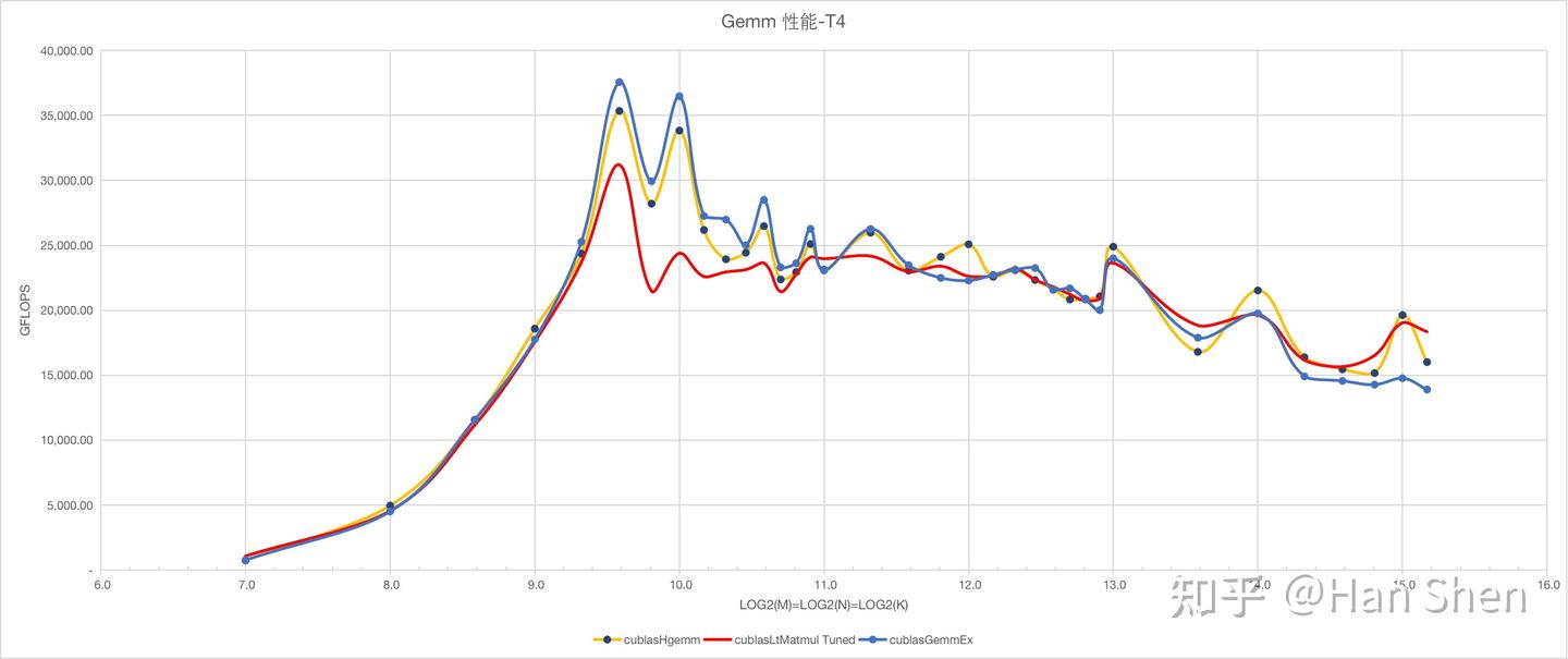
T4 FP16 square-matrix GEMM performance
The largest test case reaches only 39 TFLOPS — 56% of rated peak. Here is the GPU state during that run, using cublasHgemm:
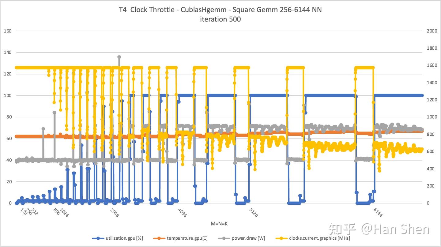
T4 cublasHgemm power and clock timeline
The x axis is time. Because this is a continuous monitored sweep with M, N and K growing over the run, the points where M changes are marked along it. There are two y axes: the primary carries GPU utilization, temperature and power; the secondary (yellow curve) carries the graphics clock.
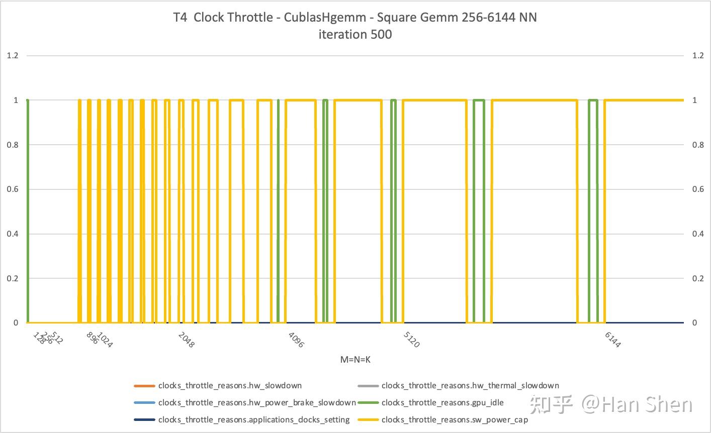
T4 cublasHgemm clock-throttle-reason timeline
From the throttle-reason timeline, the T4 begins asserting sw_power_cap at around M = 768. On the power and clock timeline, the grey power curve repeatedly reaches beyond 70 W, and the yellow clock curve begins dropping frequently. As matrices grow further, sustained power holds around 70 W, throttling fires continuously, the graphics (SM) clock falls from 1590 MHz to below 800 MHz, and achievable throughput declines with it. Notably, M = 768 — the point where throttling begins — is exactly where the T4's GFLOPS curve peaks.
One oddity: cublasLt delivers noticeably lower GFLOPS than cublasHgemm and cublasGemmEx between M = 768 and M = 2048. Its power and clock timeline shows a similar magnitude of downclocking over that range, but each shape is preceded by a tuning phase, and different algorithms trigger throttling to different degrees — which may interfere with cublasLt's algorithm selection. The baseline temperature was also higher during this run than during the cublasHgemm run, so I cannot say for certain whether that contributed.
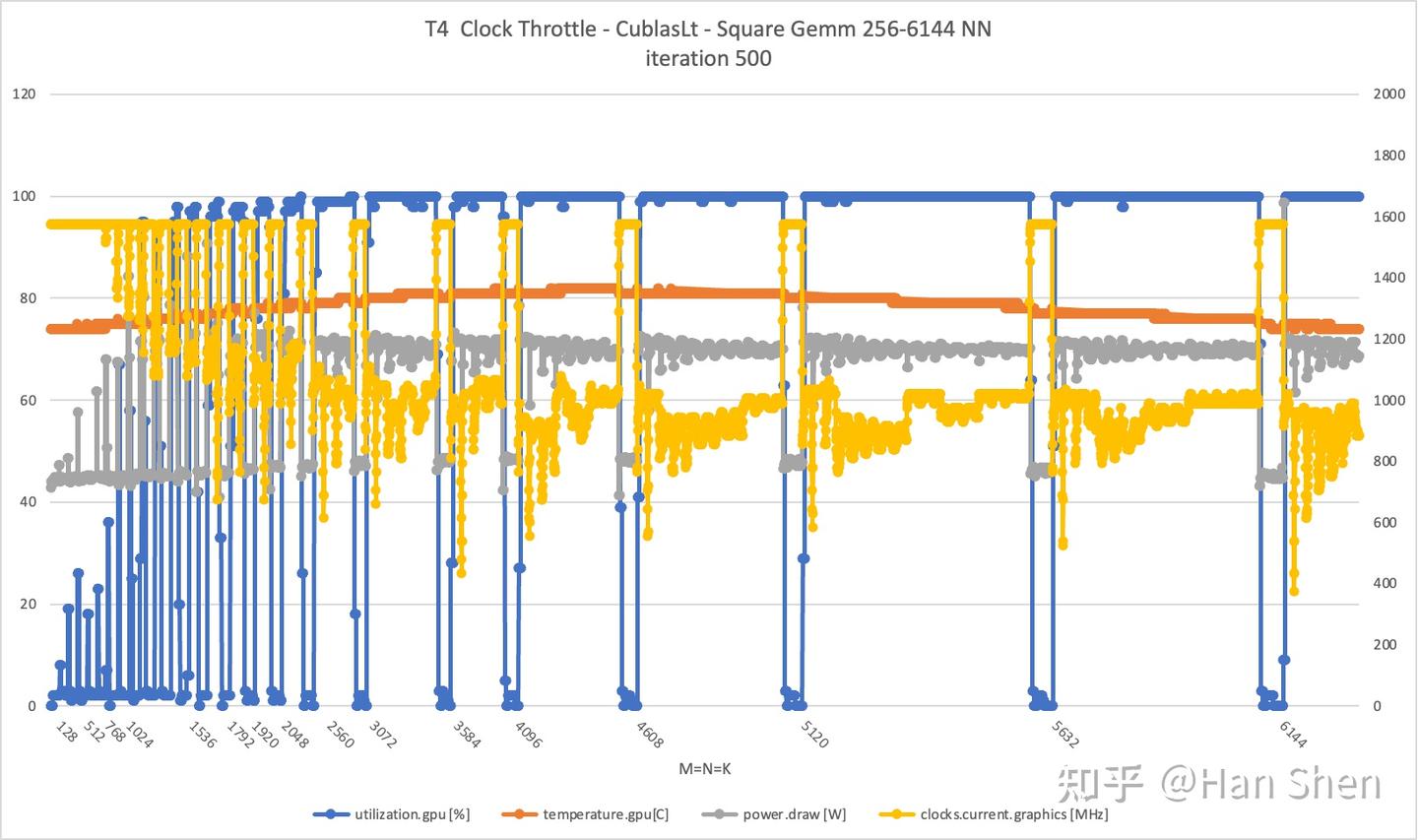
T4 cublasLt with algorithm tuning — power and clock timeline
The same method applied to the A10:
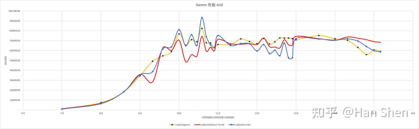
A10 FP16 square-matrix GEMM performance
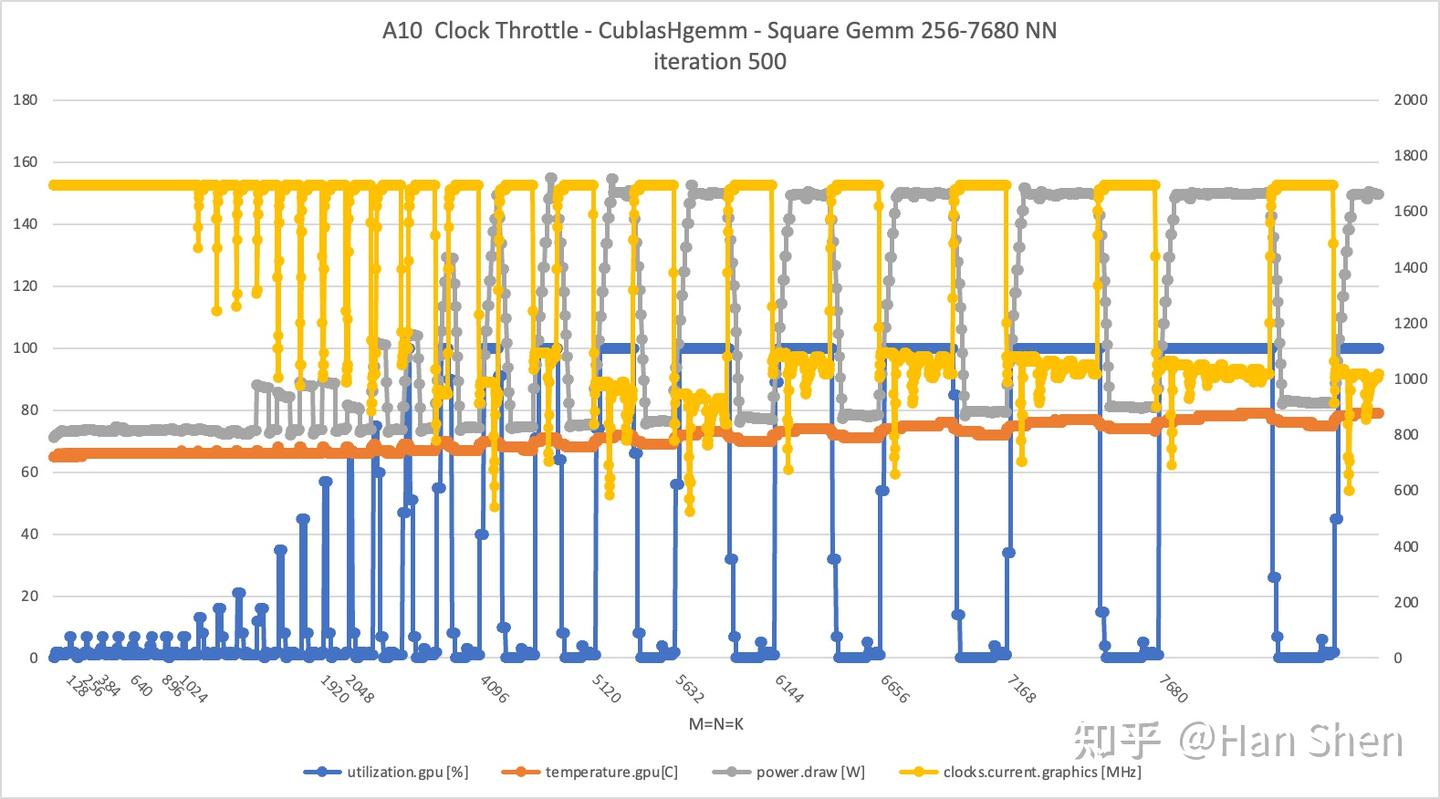
A10 cublasHgemm power and clock timeline
The A10's power limit sits around 150 W, and its temperature stays lower than the T4's — within 80 °C. Throttling here can therefore be treated as temperature-independent and driven purely by TDP, via sw_power_cap. Compared with the T4, the onset of throttling is delayed to M = 1024.
Summary
Because of sw_power_cap, neither the T4 nor the A10 comes close to its rated compute. The T4 is especially poor, reaching 56% of peak — for anything beyond a small model, compute saturates almost immediately. Even setting large models aside, MFU figures for conv/transformer/MLP networks on the T4 look considerably less favourable once this is accounted for.
| T4 | A10 | |
|---|---|---|
| FP16 peak (TFLOPS) | 65 | 125 |
| Memory bandwidth (GB/s) | 300 | 600 |
| Power (W) | 70 | 150 |
| Best measured TFLOPS | 39 | 95 |
| Best measured as a fraction of rated peak (peak MFU) | 56% | 76% |
Results: A800 / H800 Reference Parts
Now the reference parts of the large-model era: A800 SXM 80G, A800 PCIe 80G, and H800 SXM.
| A800 SXM | A800 PCIe | H800 SXM | |
|---|---|---|---|
| FP16 peak (TFLOPS) | 312 | 312 | 989 |
| Memory bandwidth (GB/s) | 2039 | 1935 | 3350 |
| Power (W) | 400 | 300 | 700 |
A800 SXM 80G
FP16 supports both FP32 and FP16 accumulators, so both call paths were tested; on Ampere the two deliver identical throughput.
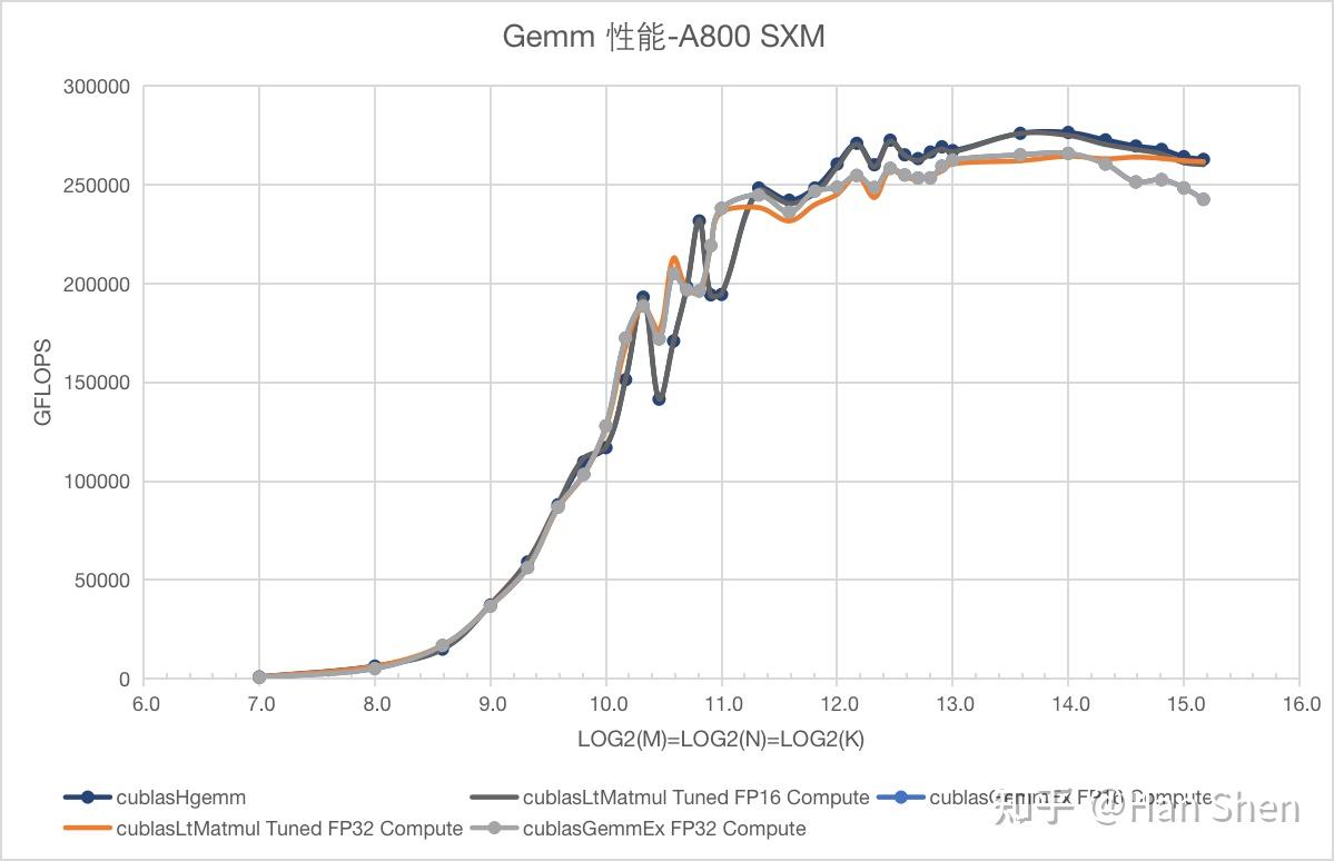
A800 SXM FP16 square-matrix GEMM performance
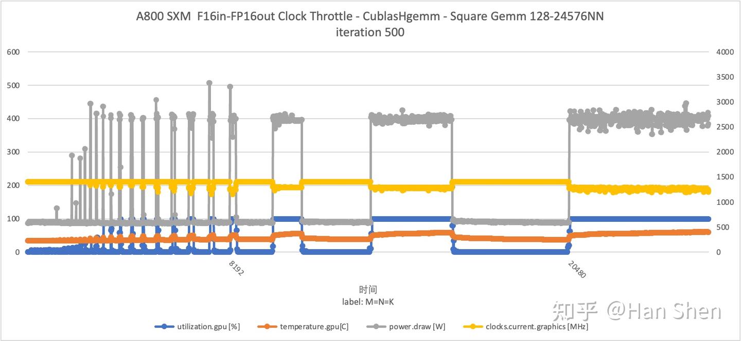
A800 SXM cublasHgemm power and clock timeline
The A800 SXM's TDP sits around 400 W, and downclocking is mild as matrices grow. Pushing the shapes larger still — well past 99% of what appears in real DNNs — does not make throttling appreciably worse, so the A800 SXM sustains high throughput even at very large sizes. It nevertheless leaves a gap to the rated spec, topping out at 89%.
The same procedure gives the A800 PCIe and H800 SXM results.
Summary
Even on the A800 and H800 — high-compute parts with relatively modest TDP for that compute — rated peak is not reached. When measuring MFU, these power constraints need to be folded into the upper bound.
| A800 SXM | A800 PCIe | H800 SXM | |
|---|---|---|---|
| FP16 peak (TFLOPS) | 312 | 312 | 989 |
| Memory bandwidth (GB/s) | 2039 | 1935 | 3350 |
| Power (W) | 400 | 300 | 700 |
| Best measured TFLOPS | 278 | 248 | 800 |
| Best measured as a fraction of rated peak (peak MFU) | 89% | 79% | 81% |
Results: Export-Compliant Parts
Finally the H20 — the compliance-sensitive measurements are omitted here. After the November 2023 export controls, the H800 was replaced by the H20 in this market. Its rated compute is only a little above the A10's, while its TDP is 500 W, far more headroom than that compute requires. As you would expect, its MFU is largely unconstrained by TDP: measurements exceed 95% of rated peak, making it the most honestly-rated part of the group. That contrast shows how much TDP design governs achievable peak performance.
Conclusions
TDP matters when comparing the peak compute of different cards, and especially when selecting hardware: you need a working notion of the performance upper bound each part can actually reach. At large matrix sizes, falling short of rated peak is not evidence that the vendor library is poorly implemented — the power design has capped further GFLOPS gains.
For anyone working on GPU or compiler optimization: when matrices are large and TDP cannot sustain the compute demand, no amount of tuning will beat the vendor kernel. That is the point to stop iterating on the schedule and look at the hardware constraints instead.